6502 + FPGA Retrocomputer
Do you ever have one of those project ideas you just can’t get out of your head until you turn it into a reality? This is one of those.
A long time ago, I started building a 6502 computer from scratch on perfboard, hand-wiring all of the buses and using 74HCXX series logic to interconnect everything. I never finished that project - I was able to get the CPU cycling and show fetch addresses on some LEDs, but never really took it any further, mostly out of a lack of time and a serious lack of patience with soldering individual wires for the data bus.
There’s a part of me that always wanted to revisit this project, perhaps using a PCB instead of hand-wiring everything, but it feels like everyone and their dog has a 6502 retro-inspired computer project kicking around, and I wanted to do something a little different.
I’ve always been fascinated by FPGAs - programmable hardware is just too cool to pass up - and I’ve been trying to improve my PCB design skills, and push the limits of my SMT assembly capabilities.
I decided I wanted to build a “brain in a jar” - a 6502 that connects directly to an FPGA to emulate all of the “normal” peripherals it might normally talk to.
I knew there were some key peripherals/functions I wanted to have on board:
- Use a real DIP-packaged 65C02 (with the ability to upgrade to a 65C816, since all the hardware is programmable!)
- HDMI output for a monitor (no VGA here!)
- USB ports for mass storage and keyboards (no PS/2 here!).
- 7 segment display for debug and general coolness.
- Two SD card slots for data and program storage.
- At least a few hundred kilobytes of RAM, with a custom MMU able to swap pages of that RAM in and out of the address space of the processor.
- Just for fun - push myself to use surface-mount parts where possible to gain experience with assembly and rework.
The goal for this project really was a learning exercise more than anything else - it was going to be my first 4-layer PCB, first multi-output switching voltage regulator, first FPGA design (!), first BGA, and first time reflowing a PCB instead of hand-soldering with an iron (more on the complexities of that last point later).
Design Stage
As with all projects, design starts with requirements. In addition to the features I knew I wanted above, there were a few other constraints I had in mind:
- The board could be no larger than 100mm x 100mm to avoid extra charges from JLCPCB.
- The board could be no more than 4 layers - 6 layers pushed it out of my price range for a silly hobby project.
- I had one shot at this. There was no option to order dev kits or put together some test boards before the real thing - the cost simply couldn’t be justified for a hobby project.
- If this was a professional project, the risk here would be too much to bear - I’d be putting together smaller test boards and/or ordering devkits for submodules like the power section and FPGA to properly evaluate options and design choices before building the expensive main board, but alas - not possible.
- As a result, I needed to be very conservative with design - ensure reworkability, add configuration resistors for almost every strapping pin, lots of test points, etc.
- I wanted to avoid directly copying any schematics or layouts from app notes or dev boards - this is a learning experience, and that means trying to figure things out from first principles and by reading documentation. While projects from others may be a starting place or help guide component selection, directly copying doesn’t help you learn and might mean you copy mistakes from others!
- In this process, I was shocked how many “bad” designs were out there that violated manufacturer guidance, included component values that don’t exist in the real world, or had huge violations of signal-integrity best practices - they probably functioned fine enough, but it was a good reinforcement of why it’s important to understand how something works. Not that my design should be evaluated with any less grains of salt :)
- I wanted to be able to assemble multiple of these to use as generic, cheap FPGA dev boards in the future. That means including headers that could be re-purposed, and planning for other uses in component selection.
Once I had some requirements down, I started in on part selection.
- CPU: WDC 65C02 (eventually 65C816) in PDIP
- Originally I thought of using the MOS version - but they require TTL / 5v signaling. The WDC 65C02 can work down to 1.8V if required.
- FPGA: Xilinx Spartan-7 XC7S15, in FTGB196C package (1mm spacing 14x14mm BGA)
- I reviewed docs I could find from Xilinx and Altera, and I preferred Xilinx’s detailed (though fragmented) documentation on the hardware design side.
- Originally, I planned on an XC7S6, the smallest FPGA Xilinx makes in the 7 series, but after looking at pricing on Mouser, an XC7S15 was somehow cheaper, despite having twice the logic cells, DSP slices, and memory. XC7S15 it was.
- Power: We need 3 rails - 1v0 for Vccint and Vccbram, 1v8 for Vccaux, and 3v3 for the IO banks, 65C02, and SRAM. We need to sequence the rails. Several options were evaluated, but I settled on a TPS65581 which has 3 output rails, in addition to a TPS37043 supervisor IC to handle power sequencing. The TPS65581 doesn’t list a maximum output capacitance, but to reduce the risk of any loop response issues with the large capacitors Xilinx recommends, I added a very small inductor to each rail to mimic a longer PCB track based on some discussions found on TI engineering forums.
- Flash: The FPGA bitstream needs 4,310,752 bits (8Mb flash). I want to be able to store a few different ROM pages if required. IS25LP016D, a 16Mb part, was selected based on Xilinx’s “7 Series Configuration” guide.
- SRAM: I knew from IO planning that I could support a RAM part with 18 address lines. So, IS61WV5128BLL, a 512KiB asynchronous SRAM was selected based on speed (10ns access times!!!) and capacity.
- Clocks: I needed to clock the 65C02 and related internal logic, and have one high-speed clock for HDMI/video output. I decided on using a Si5351a clock generator IC, which can synthesize any frequency from ~10KHz up to ~160MHz on each of 3 outputs. The standard thing to do in these designs seems to be to drop down a 100MHz oscillator and use the PLLs within the FPGA to synthesize other frequencies - unfortunately, the PLLs on the FPGA I chose had a minimum speed of 5MHz - and I wanted to be able to clock the 6502 at 10s of kilohertz during the bringup phase. By using a programmable clock generator, I can produce whichever frequencies I want for the 6502 and the higher-speed FPGA logic (like video generation). The one catch - it requires configuration over I2C before it begins functioning. This makes board bringup slightly challenging.
- Programming: Xilinx sells “platform cables” that are incredibly expensive. Luckily, you can use an inexpensive FT232H breakout instead (there are a few other options - but you cannot use a “standard” FTDI cable.) I decided to use a breakout instead of including the adapter directly on the board to avoid debugging the debugging tools - a truly terrible state for any hardware project.
- USB Co-Processor: In order to support USB, something was going to need to handle running a USB host stack. This theoretically could have been a MicroBlaze core running on the FPGA, but I didn’t want to give up that many Block RAMs and FPGA logic fabric area. I decided to use an ATSAMD21 CPU, which supports USB device or host capabilities, paired with the tinyusb USB stack.
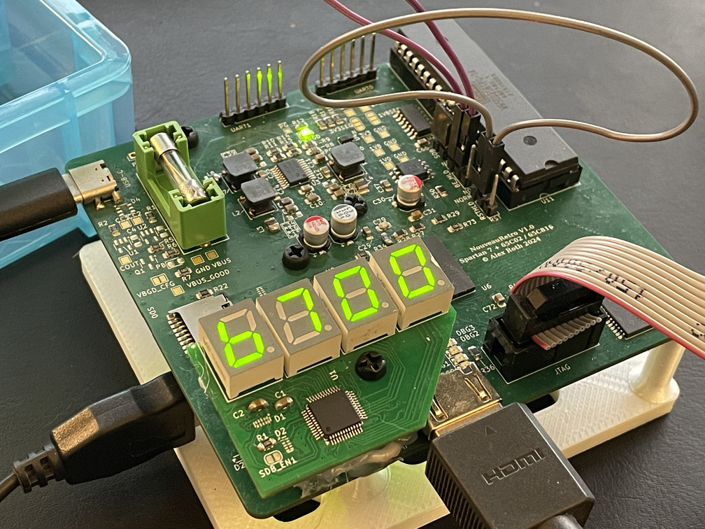
- Display & Debug: I wanted 4 LEDs directly on the board for debugging early bring-up problems. In addition, I wanted some 7 segment displays to display addresses or other hex values coming from the CPU. I decided on a IS31FL3236A 36-channel constant-current LED driver because it was the cheapest option with enough channels. It’s controlled using i2c.
I learned a lot through this design phase of the requirements of FPGAs, designing buck converters, and how (not?) to lay out and route BGA packages.
I quickly realized after schematic design that there was no way to fit everything on one 4 layer PCB (with components large enough for hand-assembly! at under 100mmx100mm. I decided to split the project up into one “motherboard” with the FPGA, 65C02, SRAM, SD card slots, and some “expansion” headers that could then connect to “expansion cards”.
I split up my schematic accordingly - designing one expansion card with the 7-segment displays and LED driver, and another using the ATSAMD21 and a USB port. I have a spare expansion port still, which I think I might use for an I2S DAC at some point.
This was the most complex electronics design project I’ve taken on yet - balancing a denser layout than I’m used to, signal integrity constraints, “fine” pitch packages, and hundreds of signal nets, many with specific impedance and timing requirements. Overall, I am happy with how the schematics and layouts turned out - there were engineering compromises made (especially around the continuity of planes on the second layer!) but for a first attempt at a multi-layer board and a BGA, I am happy.
Assembly
I designed and 3d-printed a stencil frame to ensure precise alignment of the solder stencil, especially with the 1mm pitch BGA pads. I did this by exporting a DXF file of the PCB edges and pads, and using the DXF file provided by JLCPCB when they created the stencil. By lining up the stencil with the PCB pads, I could fairly easily create a frame to hold the board in alignment with the stencil. In retrospect - slightly overkill, but it worked!
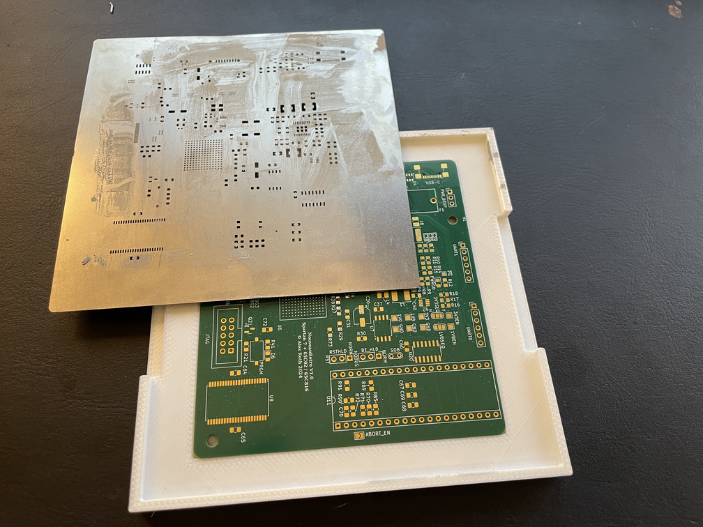
Soldering stencil frame!
I don’t have pictures of the assembly process, unfortunately, since I was too stressed with getting everything placed and baked to document it.
I did two runs of these boards - the first one had just the power section populated - I wanted to make sure the rails came up correctly and wouldn’t immediately fry the sensitive FPGA. It was also useful to supply power to the two other modules. The first run went well, and power rails were good (sort of - see Mistakes, below.)
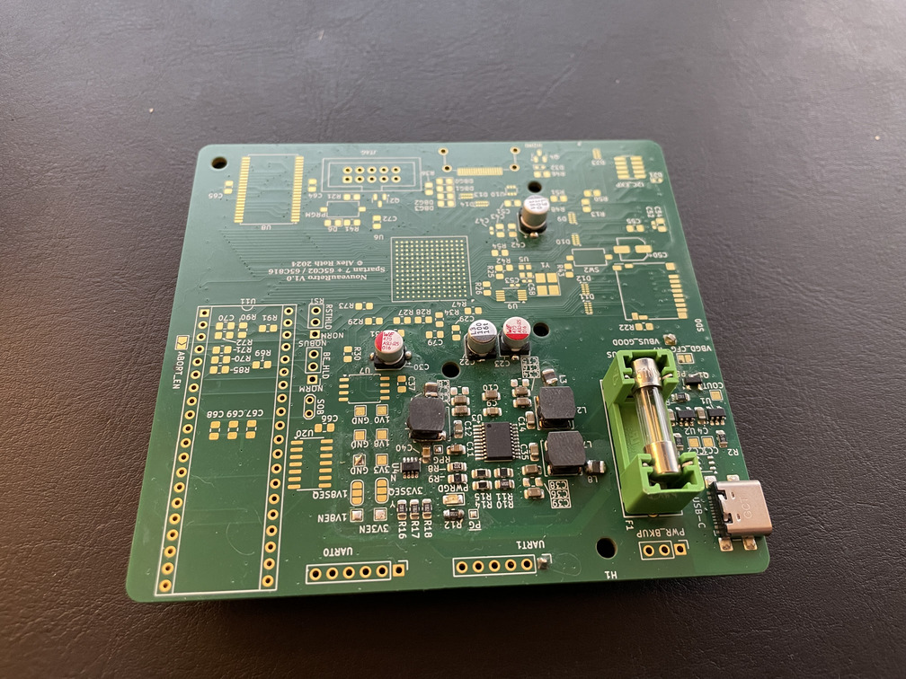
Just power components soldered on
For both boards, after placement on one side, it was baked in a re-purposed convection toaster oven. This was a bit of an adventure - I hadn’t worked with lead-free solder paste before, but the BGA balls on the FPGA were lead-free - and I didn’t want to risk using leaded paste with it’s lower melting point where the BGA balls themselves wouldn’t actually reflow.
In the end, it did work out well - a few small bridges on some of the footprints, some touchups needed on the HDMI connector and USB-C port (the problem there actually seemed to be not enough paste!). Most importantly, after applying power, seeing the “power good” LED light up, and hooking up a JTAG adapter… it immediately enumerated in the JTAG chain. The FPGA was alive!
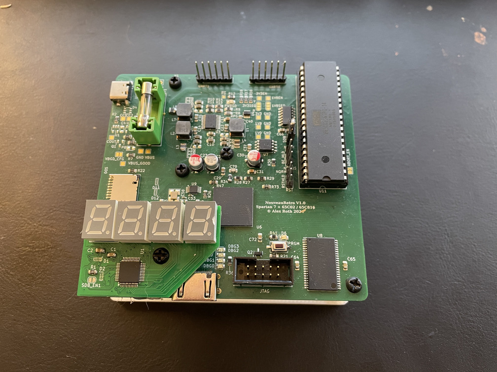
Fully assembled board!
A second 3D print was made to act as a holder for the board - it aligns with the mounting holes on the various components and has magnets in the bottom to stay on my (steel) desk pad even with cables attached.
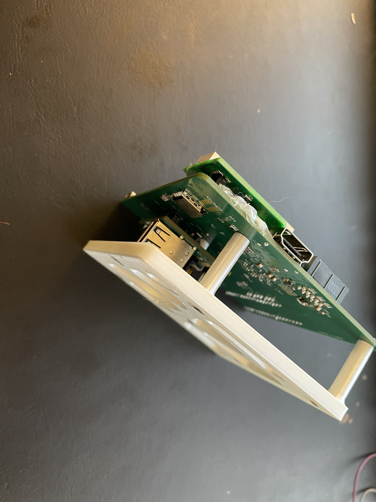
A frame to help hold everything
Bringup
Bringup of a new board with unfamiliar components is always a complex task - slowly trying to determine if the problem is the board, or your broken code. I started with simple programs on the various boards - simple hello-worlds over serial on the ATSAMD21, blinky on the FPGA (using it’s internal configuration clock - wildly inaccurate but it’ll always work!), slowly moving up the stack and adding more functionality and interfacing with more of the components.
The first big step after proving everything was soldered correctly was bringing up the programmable oscillator. This device requires i2c to configure it before it starts outputting any clocks. I used a Picoblaze soft-microcontroller to implement an i2c controller for both this and the 7 segment display. I’d like to go back and reimplement this as a VHDL IP, but it allowed for faster iteration while in the early debug phases.
Once I had clocks up and a way to output some debug information, I worked through the rest of the peripherals one at a time, proving them out.
Eventually it came time to actually bring up the 6502!
6502 Interfacing
The 6502 interfaces with the FPGA through it’s address and data lines (the other control signals are also connected by the FPGA, but most aren’t used at this point). The SRAM is also on the same bus, though the high 7 address lines and chip/write enable lines are connected to the FPGA.
I implemented some simple combinational logic to gate SRAM access based on the 6502 bus cycle - but the most interesting part is how to wire up logic within the FPGA fabric to the bus.
Read cycles are “easy” - just grab the data you need and put it on the data output pins. A dedicated “mux” IP handles ensuring it is put on the databus pins for just long enough to meet the 65C02’s hold time requirements without causing bus contention.
Write cycles (and read cycles that interact with block RAMs or other components with a synchronous, delayed/pipelined interface) require slightly more care, due to the way the 65C02’s bus interaction works.
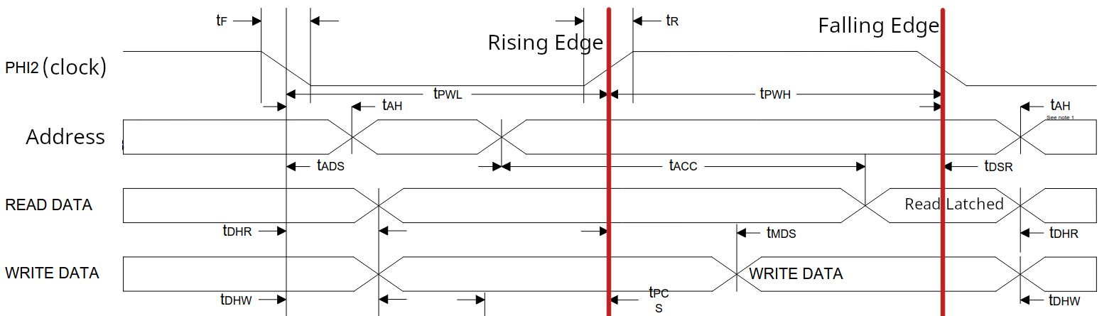
From WDC’s 65C02 datasheet, with some alterations.
This is a simplified view of the 6502’s memory bus timing diagram, from the datasheet. A single bus cycle consists of a rising edge and a falling edge of the main clock (called PHI2). On the rising edge, address lines are valid (and can be latched into external logic, including the FPGA). However - when writing data to memory, the CPU will not have valid data on the data lines yet! This diagram shows that valid write data won’t guaranteed to be present until some time after the rising edge. The most reliable time to latch it in is on a falling edge of the clock.
It’s tempting, then, to clock all of our FPGA logic on the falling edges of PHI2 - then when the 6502 writes data, we can latch in the address and data at the same time and implement our logic. Unfortunately, the 6502 expects to read data at the falling edge. This means if the FPGA was clocked on the falling edge of the clock, it wouldn’t have time to prepare data for the 6502 to read before the CPU latched whatever was on the data lines.
To handle this, I decided to use wait states. A wait-state tells the CPU to (simplifying here) pause for as long as the wait signal is in effect. When we drive the RDY line, the CPU will effectively ignore the falling edge of the clock, and keep everything on the bus in the same state. Critically, though, the data being written will still appear on the data lines in time for the next rising clock cycle.
Each FPGA component is clocked on the rising edge of PHI2. If the CPU is trying to read data, everything is easy - the component simply puts the requested data on the bus lines, and the 6502 will latch it in when the clock falls again. If the CPU is writing data, we need some special handling to capture the value being written. We can use a wait state (the RDY signal) for this purpose - if we assert RDY shortly after the clock rises, the CPU will ignore the falling edge, and on the next rising edge, our logic can latch in the data being written and release the RDY line.
For the original NMOS 6502, this wouldn’t have worked at all - write cycles ignored the ready/wait signal. But the WDC 65C02 does respect the RDY signal for both write and read cycles.
This does mean that access to some FPGA peripherals is “slow” - a full extra clock cycle. In practice for what I’m doing, it’s fine, but not ideal. The simplification is more than worth the slight slowdown in my mind. The beauty of using an FPGA to implement all of these peripherals is that if I do find a more elegant solution to this problem (or want to experiment with things like making the design synchronous to the falling edge of the clock), I can update the logic for each IP without needing a hardware re-spin!
Peripherals
I’m intending to write more about this at some point when I get more implemented, but I started with a simple set of input/output peripherals:
- A ROM implementation that uses a block RAM inside the FPGA to provide read-only access to the 6502 program - this allows updating the system through bitstream changes only, no re-programming EEPROMs!
- A simple UART used for debugging, supporting both TX and RX.
- An implementation of the USB coprocessor to handle keyboard input
- Access to an SD card on a block-by-block basis. This one is still in development, but the intention is to provide read/write access to a block of an SD card at a time by the 6502.
- A very simple character graphics display, which outputs a “framebuffer” of characters to a monitor connected over HDMI.
I have a long way to go still, but this was enough to do the first demonstration of everything working - typing a message on a USB keyboard and having it appear on an HDMI display!
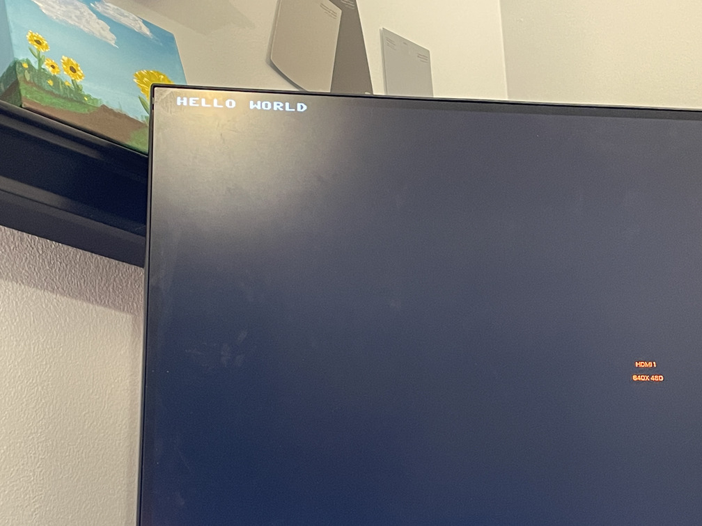
Video output working!
I hope to get back to this project soon to finish implementing the gateware and 6502 code. My goal at the moment is to run BASIC and support loading programs from SD cards.
Mistakes
This project has gone remarkably smoothly so far. But it wouldn’t be a hobby electronics project if there wasn’t at least a few bugs with the first board! This is why professionals review each other’s designs… all of these problems could have easily been caught at the design stage with some fresh eyes and some more patience.
In particular:
- Somehow I managed to mirror an N-channel MOSFET component in the power section schematic without realizing it, which I then copy-pasted into the HDMI hot-plug detect. This led to the drain and source being swapped - which is fine enough when the FET is on, but allows current to flow through it’s body diode even when off.
- This was fixable through some bodge wires - by rotating the MOSFET and soldering down the gate pin, I was able to add some wires to swap the drain and source pin, resolving the issue.
- The USB-C allowable current detection circuit did not work at all - it’s just always saying the allowed current draw is acceptable. I think this might be because I have the comparator pins backwards, but I haven’t spent much time investigating it - this was just a fun thing to try with some otherwise unused board space.
- This was a mistake I planned for in the design phase - including a solder jumper that could be cut to remove the current detection circuit from the power system entirely.
Otherwise - I have been able to bring up all the peripherals and boards without issue!
Design files
Schematics and board designs are available on GitHub here. VHDL and 6502 logic will be shared “soon”, once cleaned up enough to be worth sharing.